Home > SMT Assembly News
The solder joints shown in Figure 1 are satisfactory, but the solder resist on the pads has resulted in a reduction in the solder volume. The resist on the board is directly related to the poor design rules used on this printed board. The correct design rules for resist apertures are a 0.002-0.003" annulus ring around the pads. This clearance is necessary to allow for misalignment on the board during fabrication.
The example in Figure 1 has been designed with resist apertures smaller than the pad size. It is worth pointing out that during wave soldering the resist on the pad may affect the visual appearance of the joints but it will not cause any problems of reliability. Using a reduced resist aperture has been used in the past by the author to eliminate solder shorting. Sometimes it is not always possible to eliminate problems simply with changes to process parameters. As an alternative, when all else fails and when the design engineer does not want to change the design, use a glue dot. Ask your placement engineers to program in an extra glue dot between the lead which always shorts, this will be a simple fixit.
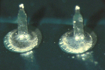
Figure 1: Here, the resist apertures are smaller than the pad size.
Keywords:
SMT Reflow Oven, Lead free Reflow Oven, Reflow Oven Manufacturer, LED reflow oven, PCB Reflow Oven, Nitrogen Reflow Oven, Dual Rail Reflow Oven, China Reflow Oven, wave soldering machine, Dual Rail Wave Soldering Machine, Nitrogen Wave Soldering Machine, Wave Soldering Machine Manufacturer.
Flason Electronic Co.,ltd provide a full SMT assembly line solutions, including SMT Reflow Oven, Wave Soldering Machine, Pick and Place Machine, SMT Stencil Printer, SMT AOI SPI Machine, SMT Reflow Oven, SMT Peripheral Equipment, SMT Assembly line, SMT Spare Parts etc any kind SMT machines you may need, please contact us for more information: wechat whatsapp:+8613691605420, Skype: flasonsmt, Email: sales@flason-smt.com

Contact: Mr Tommy
Phone: +86 13691605420
Tel: +86 -755-85225569
Email: sales@flason-smt.com
Add: No.94,Guangtian Road,Songgang Street,Bao an District Shenzhen China