Home > SMT Assembly News
Lifted components can occur during wave soldering for a number of reasons. In the case of Figure 1, the part lifted due to the thermal demand on the leads. Simply by increasing the immersion time in the wave eliminated the problem. On lambda style waves it is possible to increase the contact time by adjusting the back wave section which eliminates the need to slow down the conveyor. Slowing down the process does not go down well with production managers. Generally components lift due to: Incorrect lead length causing the leads to hit the solder bath and lift during entry to the wave. Flexure of the board which is commonly seen on large connectors, IC sockets or large IC packages. Basically the board flexes and the component remains still. Light components are lifted by the turbulent wave used for surface mount applications. Components with either different thermal demands or different lead solderability can also cause the lifting seen during wave contact. Although not associated with the wave, vacuum formed shrinkwrap may cause lifting during wave contact. The shrink wrap is some times used to hold components on the surface of the board for lead cutting. It can be pulled under the leads which causes components to lift during wave contact.
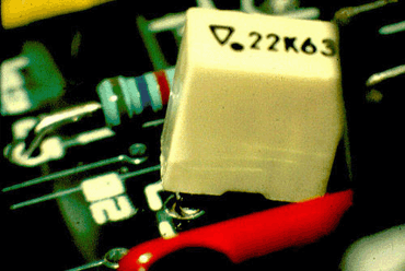
Figure 1: Increasing the immersion time in the wave stopped this problem from occurring.
In the case of Figure 2, the part was not inserted correctly prior to entering the soldering process. It is uncommon for IC packages of this size to lift during wave contact. Generally components lift due to: Incorrect lead length causing the leads to hit the solder bath and lift during entry to the wave. Flexure of the board which is commonly seen on large connectors, IC sockets or large IC packages. Basically the board flexes and the component remains still. Light components are lifted by the turbulent wave used for surface mount applications. Components with either different thermal demands or different lead materials. If a lead is slow to wet due to the thermal demand of the component it can lift in the plated through hole and not sit back on to the surface of the board.
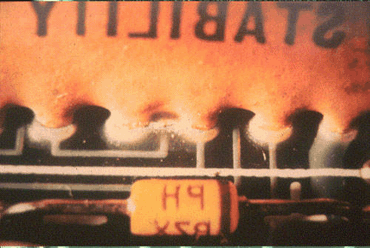
Figure 2: This defect originated in the assembly process, when the part was inserted incorrectly.
Keywords:
SMT Reflow Oven, Lead free Reflow Oven, Reflow Oven Manufacturer, LED reflow oven, PCB Reflow Oven, Nitrogen Reflow Oven, Dual Rail Reflow Oven, China Reflow Oven, wave soldering machine, Dual Rail Wave Soldering Machine, Nitrogen Wave Soldering Machine, Wave Soldering Machine Manufacturer.
Flason Electronic Co.,ltd provide a full SMT assembly line solutions, including SMT Reflow Oven, Wave Soldering Machine, Pick and Place Machine, SMT Stencil Printer, SMT AOI SPI Machine, SMT Reflow Oven, SMT Peripheral Equipment, SMT Assembly line, SMT Spare Parts etc any kind SMT machines you may need, please contact us for more information: wechat whatsapp:+8613691605420, Skype: flasonsmt, Email: sales@flason-smt.com

Contact: Mr Tommy
Phone: +86 13691605420
Tel: +86 -755-85225569
Email: sales@flason-smt.com
Add: No.94,Guangtian Road,Songgang Street,Bao an District Shenzhen China